
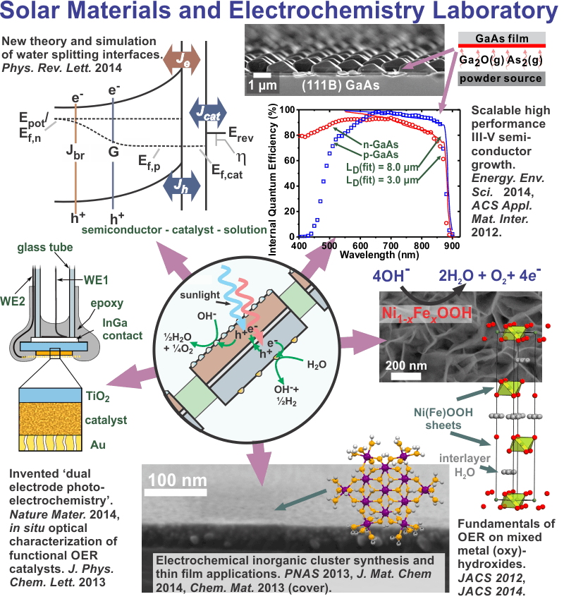
Overview
The Boettcher inorganic materials photoelectrochemistry laboratory is focused on designing, synthesizing, and understanding materials for applications in solar energy conversion and storage. Specific interests include the synthesis and study of heterogeneous electrocatalysts for water oxidation with defined molecular and nanoscale structures, the use of computer simulation and direct electrical measurements to understand semiconductor-electrocatalyst interfaces, and the development of high-performance III-V semiconductor solar conversion architectures using scalable and inexpensive deposition processes.
Video Seminars Delivered by Prof. Boettcher
Water Dissociation Catalysis in Bipolar Membranes and for Electrocatalysis
20 min talk on water dissociation in bipolar membranes and electrocatalysis
Introduction and Motivation
The continued prosperity of our current civilization will require replacing fossil fuels with renewable, sustainable, and carbon-free energy sources. More energy hits the earth in the form of sunlight in one hour than civilization uses in one year. Current photovoltaic (PV) technology will likely reach “grid-parity” (10-15 ¢ kW^-1^ hr^-1^) and drive continued commercial PV growth in the near term.1 Long-term, the critical unsolved challenge of storing massive amounts of energy derived from intermittent renewable sources such as the sun, will limit PVs to providing less than 20-30% of the electricity supply.2 Furthermore, electricity constitutes less than 15% of total energy use worldwide. A replacement for the remainder, i.e. the energy-dense fossil hydrocarbons used in transportation, to heat homes, and to run factories, is also critical.
The development of inexpensive and scalable materials systems that directly convert sunlight into an energy-dense chemical fuel would enable the storage, and hence utilization, of solar energy on a massive scale. The simplest chemical fuel is H2, which could be derived from the photochemical splitting of water and later used in a fuel cell, burned like natural gas, or used as a feedstock to make methanol from CO2. One promising technological vision for a solar water-splitting system is depicted in Figure 1. Such as system utilizes two semiconductors in series.3 These semiconductors absorb light and separate electron-hole pairs. The electrons are shuttled to a catalyst and then used to reduce protons to H2 gas. The positive holes are shuttled to a different catalyst material and used to oxidize H2O to O2 gas and H2. A polymer sheet could be used to both hold the components in place and separate the H2 and O2 gas. Because the excited electrons and holes are used to drive chemical reactions at the semiconductor /catalyst surface, no wires or complicated 3D contacting schemes are needed. These features could lower the costs of water splitting systems compared to traditional photovoltaic systems, while also providing for energy storage in the form of H2. To build such a system and make it efficient, we must develop and understand the fundamental properties of catalysts and semiconductors, as well as the interfaces between them.
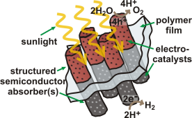
Figure 1. One vision for a solar water-splitting cell that utilizes only sunlight and water as inputs and generates H2 and O2 products. Researchers around the world are working on various fundamental and applied aspects of similar “devices”.
(1) Nemet, G. Learning Curves for Photovoltaics., International Energy Agency, 2010.
(2) Lewis, N. S. Powering the planet. MRS Bulletin 2007, 32, 808-820.
(3) Walter, M.; Warren, E.; McKone, J.; Boettcher, S. W.; Qixi, M.; Santori, L.; Lewis, N. S. Solar Water Splitting Cells. Chem. Rev. 2010, 110, 6446-6473.
Semiconductor-electrocatalyst contacts: theory, experiment, and applications to solar water photoelectrolysis
Semiconductor photoelectrodes coated with electrocatalysts are key components of photoelectrochemical (PEC) energy conversion and storage systems. Despite an intense effort aimed at optimizing these materials, there has been little systematic work focused on the semiconductor-electrocatalyst (SC-EC) interface. The SC-EC interface is important because it responsible for collecting the photoexcited electron-hole pairs generated in the semiconductor. The objectives of this research are to: (1) Understand the rate-/performance-limiting processes at SC-EC interfaces using computer simulations to predict PEC J-E response as a function of materials parameters. (2) Fabricate and study model systems using single-crystal photoelectrodes to verify predictions and determine how the rates of SC-EC electron/hole transfer and the SC-EC interface energetics vary for different catalyst architectures. The catalyst architectures that are studied include dense crystalline oxide films, redox-active ion-permeable oxide/hydroxide films, and monolayers of robust inorganic molecular catalysts. (3) Uncover the interface/catalyst design-principles critical to improving PEC water-splitting photoanodes.
This work focused on SC-EC interfaces will therefore fill key knowledge gaps in the understanding of solar-water-splitting using catalyst-modified semiconductor photoelectrodes. This will enable the design of improved materials systems that are practically relevant because they provide a mechanism to directly convert and store solar energy in the form of hydrogen gas, a renewable chemical fuel.

Enabling High-Efficiency GaAs Photovoltaics Grown via Vapor Transport from a Solid Source
GaAs is an attractive material for high-efficiency photovoltaics, but its widespread implementation is limited in part by the high cost of metal-organic chemical vapor deposition, which employs toxic and pyrophoric gas-phase precursors. We study the growth of GaAs by close-space vapor transport (CSVT), which uses solid GaAs as a source and water vapor as a transport agent as an alternative, and possibly low-cost, technique for depositing GaAs films. Epitaxial n-GaAs thin films were grown on n+-GaAs substrates while varying the water vapor concentration and the source/substrate temperatures. The photovoltaic properties of the films were evaluated using a non-aqueous photoelectrochemical test cell containing the ferrocene/ferrocenium redox couple.
Remarkably, we found little dependence of the photovoltaic response on the water content used to grow the films suggesting that the incorporation of oxygen-related defects from the water may not limit the materials performance. With 100 mW cm-2 of AM1.5G solar simulation incident on the front surface of the test cell, the best electrodes yielded Jsc = 16-17 mA cm-2, ff = 0.64, Voc > 820 mV, and efficiency ~ 9 %, which was significantly better than high-quality commercial n-GaAs wafers (efficiency ~ 7 %). After correction for reflection losses the spectral response was analyzed to determine the minority carrier diffusion length which for the best films was ~ 1.5 µm compared to ~ 0.7 µm for the commercial wafers. Device-physics modeling shows that solid-state devices could have AM1.5 solar efficiencies as high as ~23% with no additional improvements in materials quality. The films are characterized via photoluminescence lifetime and secondary ion mass spectrometry measurements in order to understand the photovoltaic properties. Current efforts include the fabrication of solid-state CSVT GaAs pn junctions, the growth and characterization of the films on alternative low-cost substrates including Mo and Si, and the introduction of controlled 3D structure for light management.

References:
Ritenour, A. J.; Cramer, R. C.; Levinrad, S.; Boettcher, S. W. Efficient n-GaAs Photoelectrodes Grown by Close-Spaced Vapor Transport from a Solid Source. ACS Appl. Mater. Interfaces 2012, 4, 69-73.
Ritenour, A. J.; Boettcher, S. W. Towards High-Efficiency GaAs Thin-Film Solar Cells Grown via Close Space Vapor Transport from a Solid Source. IEEE PVSC 38, 2012.
Thin-Film Mixed Metal Oxide and Hydroxide Oxygen Evolution Electrocatalysts: Fundamentals and Applications
The slow kinetics of the oxygen evolution reaction (OER, in basic media: 4OH– → 2H2O + O2 + 4e–) limit the performance of promising large-scale energy technologies based on the photo-driven or electricity-driven production of H2 from water (H2O → H2 + ½O2).1,2 The longstanding challenge is that the active catalysts typically studied are poorly defined, which makes relating structural, compositional, and electronic features to the observed catalysis behavior difficult, especially on heterogeneous surfaces.
We recently demonstrated higher intrinsic OER activity for thin films of Ni-Fe based layered hydroxides/oxyhydroxides [abbreviated as (oxy)hydroxides] than for other known electrocatalysts in alkaline solution and are now working to study these structures in detail.3 Divalent cations (e.g. Mg, Ca, Mn, Fe, Co, Ni) can form hydroxides which are composed of 2D sheets of covalent µ3-hydroxo-bridged metals with the layered-double-hydroxide “brucite” structure (Figure 1). The sheets are held together by non-covalent interactions allowing for the movement of water and ions between the sheets and throughout the structure when it undergoes redox chemistry. The oxidized NiOOH sheets are electronic redox conductors4 and galleries between sheets provide possible pathways for OH– transport.5
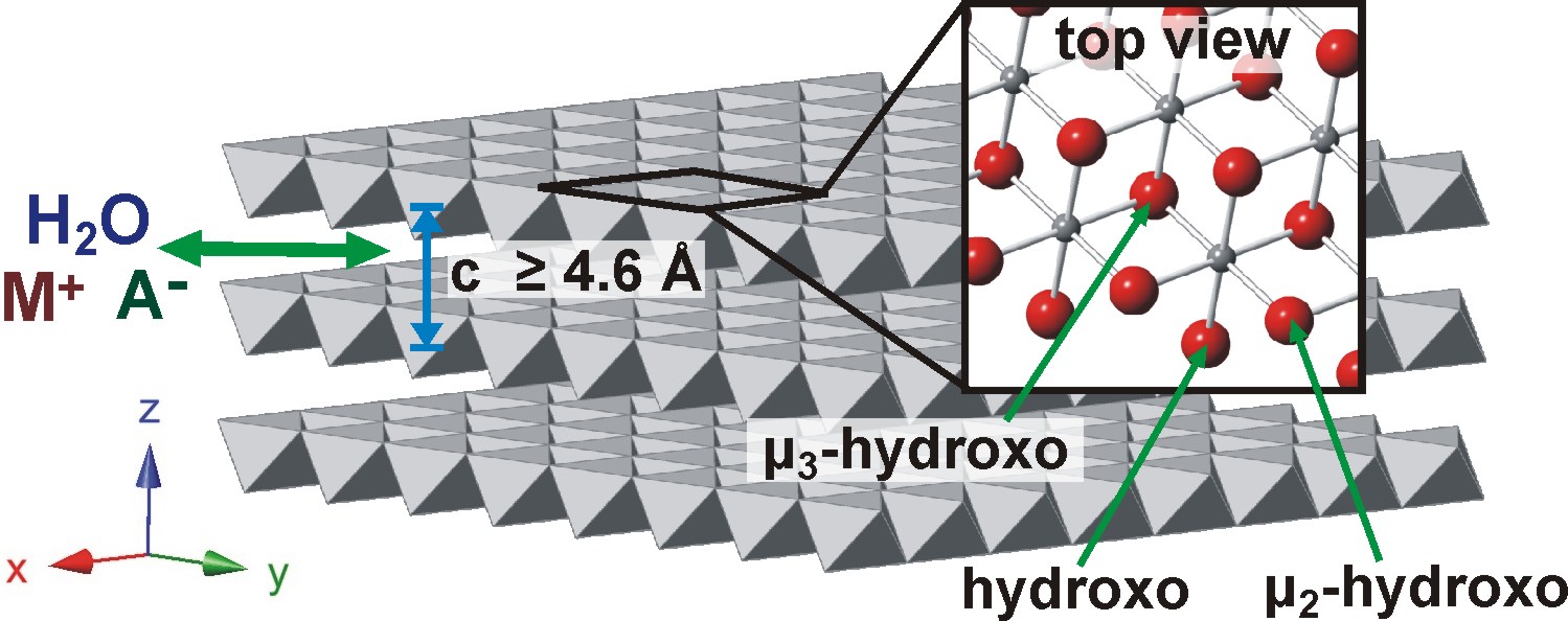
Figure 1. Ni(OH)2/NiOOH structure. The crystalline structure shown above is b-Ni(OH)2. Structures with larger sheet spacing and turbostratic disorder are known as the a-Ni(OH)2. The edge of the sheets are likely terminated with hydroxo and m2-hydroxo groups that are under-coordinated relative to the “bulk” m3-hydroxo bridges. Ions can move in-between the sheets.
We hypothesize that the layered structure of the hydroxide catalysts are especially active because the catalytic sites are sandwiched in-between redox-active transition-metal-cation sheets that modify the energetics of the reaction intermediates differently than is possible on the surface of a dense oxide and that added impurities (e.g. Fe) play a role in this 3D stabilization mechanism. Using synthesis, detailed electrochemical and structural characterization, and theory we are working to address key knowledge gaps surrounding the OER mechanism in these 3D materials and their application in practical devices: How does the sheet spacing influence the electrochemical kinetics and rate determining steps? Is the interior of a Ni hydroxide particle more or less active than the surface? Does the OER mechanism depend on impurities such as Fe in the sheets or do these impurities only affect the electrical or ionic properties? How can these catalysts be electronically and ionically “wired” into advanced alkaline-membrane-based electrolysis systems? Are the catalysts durable in practical operating environments and, if not, can the degradation mechanisms be addressed? To facilitate these efforts we have initiated collaborations with with Profs. Guenter Schneider and Líney Árnadóttir at Oregon State University who are experts in density functional theory calculations as well as with Proton OnSite, the leading manufacturer of commercial high-performance water electrolysis systems.
References:
(1) Cook, T. R.; Dogutan, D. K.; Reece, S. Y.; Surendranath, Y.; Teets, T. S.; Nocera, D. G. Solar Energy Supply and Storage for the Legacy and Non-Legacy Worlds. Chem. Rev. 2010, 110, 6474-6502.
(2) Walter, M.; Warren, E.; McKone, J.; Boettcher, S. W.; Qixi, M.; Santori, L.; Lewis, N. S. Solar Water Splitting Cells. Chem. Rev. 2010, 110, 6446-6473.
(3) Trotochaud, L.; Ranney, J. K.; Williams, K. N.; Boettcher, S. W. Solution-Cast Metal Oxide Thin Film Electrocatalysts for Oxygen Evolution. J. Am. Chem. Soc. 2012, Accepted, DOI 10.1021/ja307507a.
(4) Natan, M. J.; Belanger, D.; Carpenter, M. K.; Wrighton, M. S. pH-sensitive Ni(OH)2-based microelectrochemical transistors. J. Phys. Chem. 1987, 91, 1834-1842.
(5) Tadanaga, K.; Furukawa, Y.; Hayashi, A.; Tatsumisago, M. Direct Ethanol Fuel Cell Using Hydrotalcite Clay as a Hydroxide Ion Conductive Electrolyte. Adv. Mater. 2010, 22, 4401.
High-performance solution processed inorganic semiconductors for large-area electronics and energy conversion devices
Solution processing is a potentially transformative technology for the large-area deposition of functional inorganic films such as transparent conducting and semiconducting oxides. Despite the great potential, solution processing of dense high-performance inorganic films at low temperature is severely limited by the available inorganic precursor chemistry. Traditionally, inorganic precursors are stabilized in solution by organic ligands and/or large numbers of counter-ions. When organics and non-functional counter-ions are combusted (following deposition) to yield the inorganic film, they leave behind porosity which reduce performance for many applications. Developing new solution precursors that circumvent the use of organic ligands, and ideally, use water as a solvent, are therefore important.
Ideal precursors for solution-processed thin films are defined by the following features: (1) they are highly soluble (~ 1 M or higher) in “green” solvents1 such as water or ethanol so that film thickness can easily be controlled in a single spin-casting step; (2) they contain a minimal number of counterions and no organic ligands that must be later removed and cause porosity, (3) they are difficult to crystallize upon solvent evaporation (i.e., are not simple salts) so that as-deposited films are smooth; and (4) they are stable yet dynamic in solution, poised to crosslink upon mild heating in the solid state to yield dense films. Aqueous all-inorganic nanoscale clusters2-8 have emerged as solution precursors for high-quality, dense, inorganic thin films with electrical properties in some cases equivalent to the best vacuum-deposited films.9-13
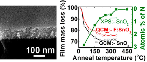
In one example we have developed new aqueous thin-film precursor based on tin(II) hydroxide nitrate clusters.14 This precursor has a number of attractive features, including low-temperature (~100 ºC) inorganic film formation that enables the deposition of conducting F:SnO2 films on flexible plastic films as well as the ability to use F as both a stabilizing ligand for the aqueous precursor and as a functional electronic dopant. The resulting films have electrical performance that is superior to other low-deposition-temperature precursors. In other work we are developing new approaches for semiconducting and conducting films of In-Ga-Zn-O films that have broad applications in macroelectronics.
(1) Capello, C.; Fischer, U.; Hungerbuhler, K. Green Chem 2007, 9, 927.
(2) Donaldson, J. D.; Grimes, S. M.; Johnston, S. R.; Abrahams, I. J Chem Soc Dalton 1995, 2273.
(3) Donaldson, J. D.; Moser, W. J. Chem. Soc. 1961, 1996.
(4) Casey, W. H. Chem Rev 2006, 106, 1.
(5) Son, J. H.; Ohlin, C. A.; Casey, W. H. Dalton T 2012, 41, 12674.
(6) Gatlin, J. T.; Mensinger, Z. L.; Zakharov, L. N.; Macinnes, D.; Johnson, D. W. Inorganic Chemistry 2008, 47, 1267.
(7) Mensinger, Z. L.; Zakharov, L. N.; Johnson, D. W. Inorganic Chemistry 2009, 48, 3505.
(8) Mensinger, Z. L.; Wang, W.; Keszler, D. A.; Johnson, D. W. Chem Soc Rev 2012, 41, 1019.
(9) Mensinger, Z. L.; Gatlin, J. T.; Meyers, S. T.; Zakharov, L. N.; Keszler, D. A.; Johnson, D. W. Angew Chem Int Ed Engl 2008, 47, 9484.
(10) Meyers, S. T.; Anderson, J. T.; Hung, C. M.; Thompson, J.; Wager, J. F.; Keszler, D. A. J Am Chem Soc 2008, 130, 17603.
(11) Jiang, K.; Anderson, J. T.; Hoshino, K.; Li, D.; Wager, J. F.; Keszler, D. A. Chem Mater 2011, 23, 945.
(12) Jiang, K.; Zakutayev, A.; Stowers, J.; Anderson, M. D.; Tate, J.; McIntyre, D. H.; Johnson, D. C.; Keszler, D. A. Solid State Sci 2009, 11, 1692.
(13) Meyers, S. T.; Anderson, J. T.; Hong, D.; Hung, C. M.; Wager, J. F.; Keszler, D. A. Chem Mater 2007, 19, 4023.
(14) Nadarajah, A.; Carnes, M. E.; Kast, M. G.; Johnson, D. W.; Boettcher, S. W. Chem. Mater. ASAP 2013.